
Linus Tech Tips Video Provides Behind the Scenes Look at Kioxia’s Yokkaichi Fab Production of BiCS FLASH 3D Flash Memory and SSDs
Kioxia America, Inc. today announced that Linus Tech Tips recently released a video from their visit to Kioxia Corporation’s Yokkaichi Plant in Japan. One of the largest and most advanced flash memory production facilities in the world, Kioxia’s Yokkaichi Plant is also a smart factory powered by cutting-edge digital infrastructure. More than 3 billion data points stream from the production lines every day, enabling sophisticated AI-driven insights that support precision manufacturing at scale.
This press release features multimedia. View the full release here: https://www.businesswire.com/news/home/20251217814141/en/
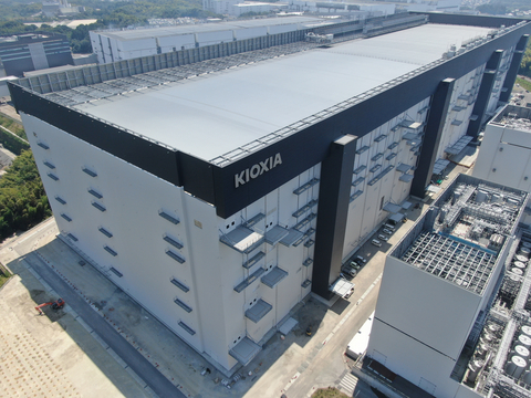
Kioxia Corporation’s Yokkaichi Plant in Japan is one of the largest and most advanced flash memory production facilities in the world.
“Bringing technology to our viewers is what drives us, and this tour inside Kioxia’s fab gives a rare, up-close look at what goes into the devices we use every day,” said Terren Tong, CEO of Linus Media Group. “We really appreciate Kioxia for letting us dive into the manufacturing of cutting-edge flash memory and SSDs.”
The newly released video has already received over 1 million views within the first 24 hours. It takes viewers on a journey with Linus Sebastian, showing how raw silicon is transformed into flash memory chips and SSDs that power the products and infrastructure we rely on every day—including laptops, mobile phones, data centers, automobiles, and countless connected devices. The tour includes rare access to Kioxia’s flagship Fab 7 (Y7), showing stages of wafer and die processing before they become KIOXIA BiCS FLASH™ 3D flash memory.
Linus highlights the remarkable engineering behind Kioxia’s 32-die stacked memory chips, demonstrating how the Y7 facility brings together advanced process controls, automation, and cleanroom discipline to deliver the reliability and performance that modern applications require. Viewers also learn what distinguishes Y7 from typical semiconductor fabs, including the highly automated material handling systems and the integration of real-time, data-driven decision making.
During a visit to one of the manufacturing lines, Linus explores how Kioxia turns individual memory dies into finished flash memory, covering everything from packaging concepts to final testing. The video then follows the journey of those memory components as they are assembled into SSDs.
“The Yokkaichi Plant is where innovation meets precision,” said Hideyuki Namekawa, president and CEO of KIOXIA America, Inc. “From the moment raw silicon enters the fab, every step is designed to deliver high-performance, reliable storage, while still being mindful of the environmental impact. We are proud to give Linus Tech Tips and viewers a rare behind-the-scenes look at the engineering, technology, and care behind our flash memory and SSD solutions that power today’s consumer devices and tomorrow’s AI-driven data centers.”
Check out the full video here: https://www.youtube.com/watch?v=ivLvsTnp9fI
For more information, please visit www.kioxia.com, and follow the company on X and LinkedIn®.
About KIOXIA America, Inc.
KIOXIA America, Inc. is the U.S.-based subsidiary of KIOXIA Corporation, a leading worldwide supplier of flash memory and solid-state drives (SSDs). From the invention of flash memory to today’s breakthrough BiCS FLASH™ 3D technology, KIOXIA continues to pioneer innovative memory, SSD and software solutions that enrich people's lives and expand society's horizons. The company's innovative 3D flash memory technology, BiCS FLASH, is shaping the future of storage in high-density applications, including advanced smartphones, PCs, automotive systems, data centers and generative AI systems. For more information, please visit KIOXIA.com.
© 2025 KIOXIA America, Inc. All rights reserved. Information in this press release, including product pricing and specifications, content of services, and contact information is current and believed to be accurate on the date of the announcement, but is subject to change without prior notice. Technical and application information contained here is subject to the most recent applicable KIOXIA product specifications.
Notes:
LinkedIn is a trademark of LinkedIn Corporation and its affiliates in the United States and/or other countries.
All other company names, product names and service names may be trademarks of third-party companies.
View source version on businesswire.com: https://www.businesswire.com/news/home/20251217814141/en/
We are proud to give Linus Tech Tips and viewers a rare behind-the-scenes look at the engineering, technology, and care behind our flash memory and SSD solutions that power today’s consumer devices and tomorrow’s AI-driven data centers.
Contacts
Media Contact:
Dena Jacobson
Lages & Associates
Tel: (949) 453-8080
dena@lages.com
Company Contact:
Mia Cool
Kioxia America, Inc.
Tel: (408) 526-3087
mia.cool@kioxia.com